
Released in 2020, the NVIDIA A100 is a data center GPU built on NVIDIA's Ampere architecture. Designed from the ground up for high-performance computing and AI workloads, it's one of the most capable GPUs for training and inference at scale.
Understanding the full set of NVIDIA A100 GPU specifications helps you determine whether it is the right hardware for your use case.
NVIDIA A100 Form Factors
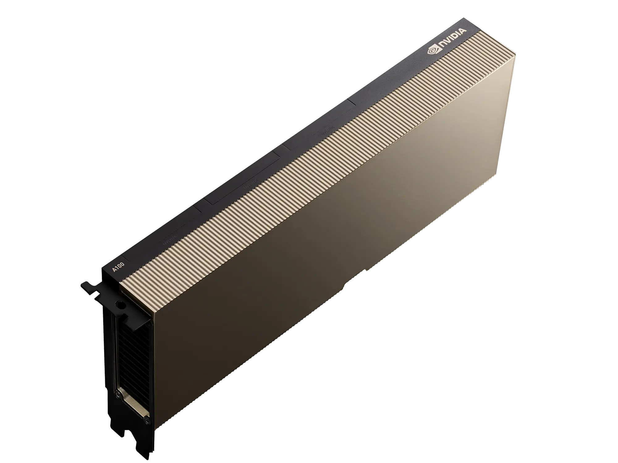
The A100 is available in two distinct form factors: PCIe and SXM. Each one targets different deployment environments, and the choice between them directly affects thermal design, bandwidth, and peak performance.
NVIDIA A100 PCIe
The PCIe variant fits into standard server motherboards using a PCIe 4.0 x16 interface. It comes in both 40GB HBM2 and 80GB HBM2e memory configurations and draws up to 300W through the PCIe slot and auxiliary power connectors.
Because it uses passive cooling and relies on server chassis airflow, it integrates easily into a wide range of existing infrastructure.
NVIDIA A100 SXM
The SXM4 variant mounts directly to NVIDIA's NVLink Switch System baseboard, enabling tighter GPU-to-GPU interconnects and a higher power envelope of 400W.
This higher thermal headroom translates directly into improved clock speeds and memory bandwidth compared to the PCIe version. The SXM form factor is the basis for NVIDIA's own DGX and HGX systems, making it the preferred choice for maximum multi-GPU throughput.
NVIDIA A100 Specifications
The table below shows key NVIDIA A100 specs across form factors and memory configurations.
| Specification | A100 PCIe 40GB | A100 PCIe 80GB | A100 SXM 40GB | A100 SXM 80GB |
|---|---|---|---|---|
| Architecture | Ampere | |||
| GPU | GA100 | |||
| CUDA Cores | 6,912 | |||
| Tensor Cores (3rd Gen) | 432 | |||
| GPU Boost Clock | 1,410 MHz | |||
| A100 VRAM | 40GB HBM2 | 80GB HBM2e | 40GB HBM2 | 80GB HBM2e |
| Memory Bandwidth | 1,555GB/s | 1,935GB/s | 1,555GB/s | 2,039GB/s |
| Memory Bus Width | 5,120-bit | |||
| L2 Cache | 40 MB | |||
| TDP | 250 W | 300 W | 400 W | |
| Interconnect | PCIe 4.0 x16 | NVLink 3.0 (600GB/s) | ||
| PCIe Bandwidth | 64GB/s | |||
| Multi-Instance GPU (MIG) | Yes (up to 7) | |||
The 80GB SXM variant delivers the highest memory bandwidth and capacity of any A100 configuration, making it the preferred choice for large model training runs where the working dataset does not fit in smaller GPU memory.
NVIDIA A100 Supported Precisions
An important part of NVIDIA A100 GPU specifications for AI is the range of precisions supported through its CUDA and Tensor Cores. Different precisions offer different trade-offs between numerical accuracy and raw throughput.
| Precision | A100 | Notes |
|---|---|---|
| FP64 (Tensor Core) | 19.5 TFLOPS | Scientific computing and HPC |
| FP64 (CUDA Core) | 9.7 TFLOPS | Standard double precision |
| FP32 | 19.5 TFLOPS | Full single precision |
| TF32 (Tensor Core) | 156 TFLOPS / 312 TFLOPS* | Default precision for DL frameworks |
| FP16 | 312 TFLOPS / 624 TFLOPS* | Standard half precision for training |
| BFLOAT16 (Tensor Core) | 312 TFLOPS / 624 TFLOPS* | Favored for LLM training stability |
| INT8 (Tensor Core) | 624 TOPS / 1,248 TOPS* | Quantized inference |
| INT4 (Tensor Core) | 1,248 TOPS / 2,496 TOPS* | Highly quantized inference |
The A100 does not natively support FP8 computation, which was introduced with the Hopper generation (H100) and its fourth-generation Tensor Cores.
NVIDIA A100 Chip
The A100 is built on the GA100 die, manufactured by TSMC on a 7 nm process node. The full die contains 54 billion transistors in a 826 mm² package, though the shipping GPU enables 108 of a possible 128 Streaming Multiprocessors (SMs) to maintain yield.
Each SM houses 64 FP32 CUDA cores and four third-generation Tensor Cores, with dedicated shared memory and L1 cache per SM totaling 192 KB per SM. A unified 40 MB L2 cache serves all SMs and helps reduce pressure on the HBM2e memory subsystem.
The chip introduced third-generation Tensor Cores capable of executing a new TF32 format that provides the numerical range of FP32 with roughly the throughput of FP16, easing migration of existing FP32 training pipelines without code changes.
It also introduced Multi-Instance GPU (MIG) technology, which partitions a single physical GPU into up to seven isolated GPU instances, each with dedicated memory bandwidth, cache, and CUDA cores. MIG makes it practical to serve multiple independent inference workloads on a single card without contention.
NVIDIA A100 Systems
NVIDIA packaged the A100 into purpose-built multi-GPU systems that take full advantage of the SXM form factor and NVLink interconnects.
DGX A100
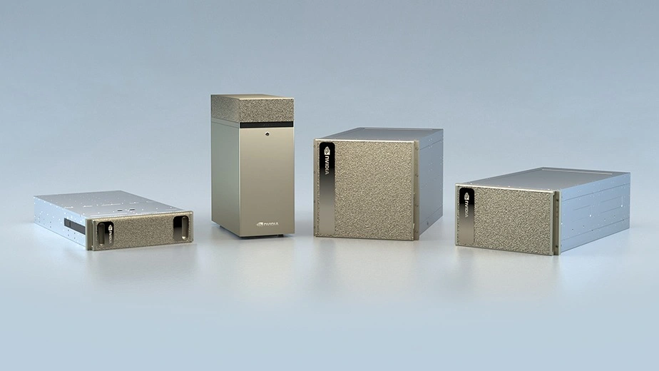
The NVIDIA DGX A100 server is NVIDIA's reference AI compute platform built around eight A100 SXM GPUs.
A full-system NVIDIA DGX A100 typically ranges from $150,000-$200,000 for new units (pricing varies based on configuration and support contracts). Secondary market units are generally available for $80,000 to $120,000.
The DGX Station A100 is the workstation variant of this design, intended for on-premises deployment where rack-mounted servers are not practical.
| Specification | Details |
|---|---|
| GPUs | 8x NVIDIA A100 Tensor Core GPUs |
| GPU Memory | 320 GB total |
| Performance | 10 petaOPS INT8 |
| NVIDIA NVSwitches | 6 |
| System Power Usage | 6.5kW max |
| CPU | Dual AMD Rome 7742 (128 cores, 2.25-3.4 GHz) |
| System Memory | 1TB |
| Networking | 8x Single-Port Mellanox ConnectX-6 VPI (200Gb/s HDR InfiniBand) 1x Dual-Port Mellanox ConnectX-6 VPI (10-200Gb/s Ethernet) |
| Storage | OS: 2x 1.92TB (M.2 NVME drives) Internal Storage: 15TB (U.2 NVME drives) |
| Software | Ubuntu Linux OS |
| System Weight | 271 lbs (123 kgs) |
| Packaged System Weight | 315 lbs (143 kgs) |
| System Dimensions | Height: 10.4 in (264.0 mm) Width: 19.0 in (482.3 mm) Length: 35.3 in (897.1 mm) |
| Operating Temperature Range | 5-30°C (41-86°F) |
HGX A100
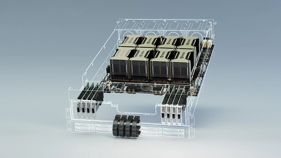
The HGX A100 is NVIDIA's OEM compute baseboard reference design, which third-party server manufacturers use to build their own A100-based systems.
Like the DGX, HGX configurations support four or eight A100 SXM GPUs connected via NVLink, but the baseboard is integrated into standard server chassis from vendors such as Dell, HPE, and Supermicro. This makes the HGX A100 the underlying hardware behind most cloud provider A100 instances, including those available on Thunder Compute.
| Specification | 4x NVIDIA A100 | 8x NVIDIA A100 | 16x NVIDIA A100 |
|---|---|---|---|
| HPC and AI Compute (FP16 Petaflops) |
2.5 | 5 | 10* |
| Memory | Up to 320 GB | Up to 640 GB | Up to 1,280 GB |
| NVIDIA NVLink | 3rd generation | ||
| NVIDIA NVSwitch | N/A | 2nd generation | |
| NVSwitch GPU-to-GPU Bandwidth | N/A | 600 GB/s | |
| Total Aggregate Bandwidth | 2.4 TB/s | 4.8 TB/s | 9.6 TB/s |
Running A100 Workloads on Thunder Compute
The A100 continues to be a strong choice for AI training, fine-tuning, and inference, particularly for mid-sized models and batch workloads where the 80GB memory tier provides ample capacity without the cost premium of newer hardware. A100 cloud pricing has become increasingly accessible as the GPU fleet has expanded across providers.
Thunder Compute offers on-demand access to A100 GPUs without long-term commitments, so you can run a large training job today and scale down when it completes. Try Thunder Compute GPUs and get your first workload running in minutes.
To match the right hardware to your workload, see our GPU selection guide for AI workflows